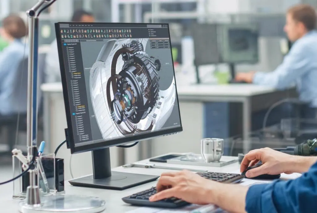


Like other fields, additive manufacturing (AM) brings numerous opportunities to the electronics industry. It integrates multiple materials into a single printing operation, which is highly beneficial for electronics. Today, 3D printing technologies are more accessible and user-friendly than ever, significantly enhancing prototyping efficiency while reducing lead times, costs, and errors that could derail production.
When to Choose 3D Printing for Electronics?
On-Demand Production
3D printing enables on-demand production of electronic components with fixed lead times and limited cost structures, drastically reducing design-to-delivery cycles. It also allows printing new or obsolete devices using various 3D printing materials from manufacturers’ digital libraries or customers’ CAD models. This advantage is transforming electronics supply chains, enabling manufacturers to meet customer needs instantly.
More Room for Innovation and Customization
Designers now have freedom to explore creative ideas without being constrained by traditional design limitations imposed by complexity. Technologies like SLS and MJF can handle intricate designs and even large-scale production—once a limitation of AM. Compared to conventional processes, AM is more efficient for mass-producing electronic enclosures, circuit boards, and other products.
For example, 3D printing solar panels allows designers to break free from traditional design rules. It optimizes both external structures and internal circuitry, enhancing component performance, reducing size, minimizing weight, and creating complex geometries.
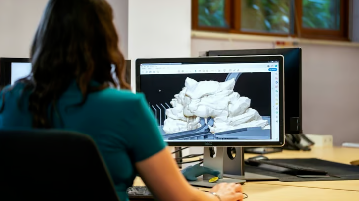
Faster Prototyping
Additive manufacturing streamlines operations and boosts efficiency, making it ideal for rapid prototyping. HP’s Multi Jet Fusion (MJF) 3D printing for nylon is cost-friendly and commonly used for prototyping.
Fused Deposition Modeling (FDM) is another prevalent AM form. Its simplicity and low printing costs make it an excellent, affordable technology for prototyping. The entire process costs less than conventional methods, enabling faster redesign and analysis cycles.
Adoption of Novel Experimental Materials
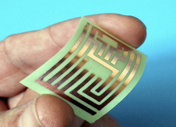
Electronics like printed circuit boards (PCBs) rely on two materials: insulating non-conductive substrates and conductive components. Recently, improved low-dielectric-constant polymers and semiconducting polymers (with tunable electrical properties) have entered use. Advanced materials combined with 3D printing open new doors for design and development.
Superior Surface Finish of Components
Stereolithography (SLA) uses liquid resin to achieve excellent surface finishes, adding flexibility and water resistance to modern electronics like foldable phones and waterproof devices. When tight tolerances and precision are priorities, SLA and similar technologies deliver.
Additionally, SLA is used for high-definition and functional prototypes.
Benefits of Additive Manufacturing in Electronics
Optimized Design
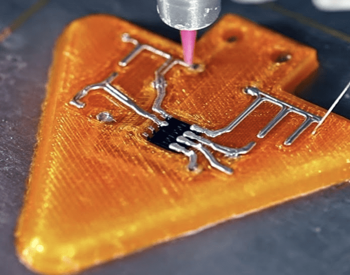
Models are created and printed digitally, minimizing errors. In traditional processes, circuits are installed after component fabrication, but AM prints circuits and components simultaneously, embedding circuits directly to protect them from external damage. For example, small antennas in mobile phones can be printed integrally with the device.
Printing on Non-Planar Surfaces
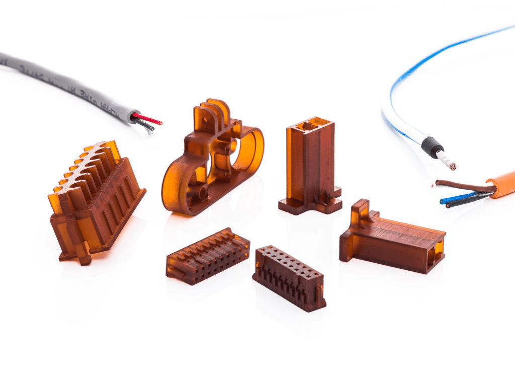
Electronics like PCBs can be directly 3D-printed on non-planar surfaces—a capability lacking in conventional methods. This allows easy integration of electronics into wearables, flexible surface sensors, glucose test strips, prosthetics, and custom batteries.
Custom devices and 3D-printed batteries are tailored to specific products and functions, outperforming conventional counterparts.
Lightweight and Reduced Material Waste
A key feature of 3D printing is material efficiency, generating less waste than traditional subtractive manufacturing—and electronics are no exception. 3D-printed electronics eliminate the need for separate wiring and extra circuits, condensing multiple production steps into a single operation for simpler assembly.
Elimination of Harmful Chemicals
Etching, which removes excess material, uses harmful chemicals. Additive manufacturing avoids this by depositing films directly, eliminating chemical use.
Conclusion
Debaolong Seiko offers online 3D printing services for prototyping and mass production projects. With over 10,000 manufacturing partners, we ensure high-quality 3D printed parts delivered to your door. Upload your 3D design files to Debaolong Seiko for a quote, and choose from a range of 3D printing services.